This writing may be considered as a very random continuation of an older post briefly mentioning the usage of photomultiplying tubes for gamma spectroscopy, but the truth is that it is so random that could be impossible to follow. I have some spare 300x600um silicon space and have been recently thinking how to fully utilize the area on the chip I am about to tapeout. Apart from having a free corner of silicon, unfortunately, time is not infinite nor free either (what?) and I have just about a week to think, analyze and engineer whatever it would be. This is why I am also posting this, hoping that in the process of writing/re-reading, I would suddenly get that brilliant idea which would vanish all first world problems and get me through academia obscura.
Back to the point. Some 5 years ago, the image sensors field suddenly realized that instead of trying to integrate the current/electrons from photo-electron pairs in the form of a stored charge on a capacitor, one could initiate an ionization process triggered by a single photon in a very high/concentrated electric field PN junction, a process often referred to as impact ionization. The last is essentially the same as the photomultiplying effect in vacuum tubes, now with the difference that the medium where the process occurs is silicon, plus some additional second order effects. The old, photon-hit-electron-integrate-readout, is a technology which has been here for decades, and still impresses us with its mature-immatureness. How is impact ionization a better solution than the conventional? The answer is – it’s not (for now), and it depends.
Here is my simple explanation of why impact ionization detectors, also called Single Photon Avalanche Diodes (SPADs) should theoretically perform better under low light conditions than the conventional technologies. In electronics, we often use the Friis formula, which states that to minimize the noise figure in a signal chain, we should apply gain in the system as early as possible, and/or perform the less noisy operations first:

It is very intuitive, and it could be applied to the signal chain of an image sensor too, even though that the signal chain begins with a noisy source of photons (photon shot noise), distorted by microlenses, attenuated by color filters, converted to electrons with noise, electrons to voltage (?) and voltage to a digital number. Most ultra low-noise CMOS image sensors use the so called High Conversion Gain (HCG) pixels. In simple language, this means that their integration capacitor (FD – floating diffusion) is minimized as much as possible compared to the photodiode junction capacitance. This results in a larger voltage swing on the integration capacitor (FD) per hit photon, which is basically equivalent to maximizing the gain at the very beginning of the photon-electron conversion process. Remember the Friis formula?
Why does a SPAD look promising for ultra-low-light imaging? Avalanche photodiodes, basing on impact ionization have an enormous gain, thus, a single photon can push the trigger causing the diode to hit the rail. Makes life easier for the rest of the measurements too, instead of a complex ADC, we can just use a counter. Sounds brilliant, however, there are some difficulties which prevent us from reaching perfect photon counting. Here’s a small list which I am thinking about right now:
- The gain in a SPAD may be considered infinite, according Friis the output should be noise-free. However, SPADs, for now, are triggered not only by photons, but also by random thermal excitation and defect traps, sudden releases and gamma ray impact with electrons. The main quality parameter of a SPAD is its so called Dark Count Rate (DCR), or false triggers per time unit under dark conditions. This is a very primitive measurement, however, until now there is no good method for quantifying what part of the DCR is caused by the respective aforementioned side effects.
- After initiation of avalanche breakdown, in order to arm the diode for another measurement round, we need to cut its power supply and then gradually apply high reverse bias voltage again. The time used for the operation is called reset time. This reset (dead) time is the major obstacle for achieving full single photon detection for high light intensities.
- SPADs work under high reverse bias voltage conditions which makes them a hard to integrate with readout electronics on 1v2/3v3 CMOS processes, while still keeping a low reset time contribution from the readout.
- SPAD structures can be easily implemented in standard CMOS and this has been done by a number of research teams during the past 5 years.
- Most of the researchers are working on SPADs for Time of Flight (ToF) imaging, or ultra-low-light sensing.
- Most of the research is done on multi-channel readout, which is actually the way to go, but is very challenging in a 2D process (no 3D stacking).
- Can we use multiple arrays, but have a single readout?
- Do we now have access to hundreds of PM tubes on a single chip? What could we use these for?
Access to hundreds of “PM tubes” on a single chip? – we call that a silicon photomultiplier (SiPM). Such have existed for a long time and are offered as discrete components, however, the information from each PM is hard to measure, all PMs share the same bus and we get a very difficult for measurement output current. Difficult, in a sense that is noisy and hard to distinguish. Conventional readout of SiPMs integrate and low-pass filter the output current before performing measurement/digitization. To grasp what I am referring to, here’s a simple electrical equivalent diagram of a SiPM:

Silicon Photomultiplier equivalent diagram
You essentially see a number of SPAD diodes with passive quench (the resistor in series) which acts as an automatic reset. When the diode fires the resulting high in-rush reverse bias current causes voltage drop on R (and the SPAD’s cathode respectively) which acts as a feedback mechanism and prevents the avalanche breakdown from continuing, thus resetting the diode by gradually increasing the cathode voltage. Typically SiPMs on the market have passive quench (resistor in series) with the SPADs, the latter are connected in parallel an could reach a relatively large number in the order of 100-1000s. The order depends on their dark and firing current and well as desired photosensitivity. To help you get an idea of how a SiPM should look physically, here’s an example of a small 8×8 SPAD array in SiPM configuration I just sketched in Virtuoso:
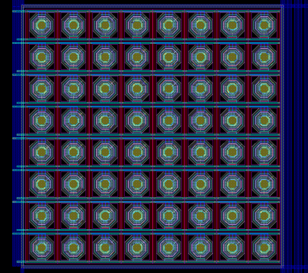
An 8×8 diode Silicon photomultiplier array layout diagram
The circular shape of the junctions comes from the fact that we want to have a strong electric field around the junction which should make the diode more susceptible to avalanche breakdown. Ideally it should be entirely circular, in the case above I’ve used hexagonal shape as this CMOS process does not alow other than 45/90 degree angles. Using hexagonal diodes generates stress electric field points which increases the dark count rate. One possible structure for SPAD formation in standard triple-well CMOS is a junction between a NW/DNW and a local P-Well created over the Deep N-Well. The latter local P-Well has the shape of a doughnut and acts as an electric field concentrator. Here’s a cross section sketch:
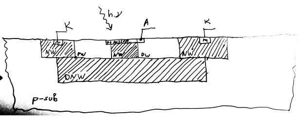
SPAD in CMOS cross-section
The thickness of the P-Well doughnut determines the strength of the electric field imposed from the N-Well surrounding doughnut to the P+ active N-Well junction. The multiplication area is formed under the island in the center of the diode. The surrounding material around the active area can be covered with top metal layers to block light and prevent PE pair stimulation outside of the intended junction. Typical SiPMs include a poly quenching resistor which surrounds the SPAD and typically have rectangular shape. In standard CMOS however, apart from the passive quench methodology, we can do all sorts of active quench circuits. What if we combine those in a SiPM? Would such a combination make the integrated current measurements easier?
The last questions remain open, likewise this random post too. Let’s see what I may come up with in the next few remaining days and hope that there would be a follow-up post containing some experimental results.
Oh, by the way, if you want to read an excellent introductory material on SiPMs, check out this link.


